Course Memo of digital IC design, including following contents:
- Basic of Design Flow
- Sequential and Combination Circuit
- Timing Issues
- Intellectual Property
- Basic of Sythesis Flow
- Clock Latency
Lec 1
Cell-based Design Flow
- Specification Development System models
- RTL code development Functional Vericication
- Synthesis Timing Verification
- Physical Synthesis/Place and Route Physical Verificatio
- Prototype Build and Test
Verilog HDL Design Flow
- Design Specification
- Algorithmic Model
- RTL Model
- Gate-Level Model
- Switch-Level Model
- Physical Layout
Data Type
4-value logic system: 0,1,x,z
Port
In a module,
- Input:
wire - Output:
reg, orwire - Inout:
wire
Useful Boolean Operators
- Bitwise:
~a,a&b,a|b,a^b,a~^b
=> bit by bit - Logical:
!a,a&&b,a||b
=> output 1 bit, high or low - Reduction:
&a,~&a,|a,~|a,^a
=> bit by bit - Comparison:
<,>,<=,>=,==,!=,===,!===
=> output 1 bit, high or low
===&!==can compare withxandzvalue.==&!=just getxif there is any unkown in comparison.
Combinational circuit
An example:
1
2
3
4
5
6
7
always @(*)
begin
if(sel)
out = a;
else
out = b;
end
Coding Style
Better to use wire for input and reg for output.
Lec 2
Sequential Circuit
Output depends not only on the current input values, but also on preceding input values.
Sequential circuit example:
1
2
3
4
5
6
7
always @(posedge clk)
begin
if(sel)
out <= a;
else
out <= b;
end
Reset
Synchronous
1
2
3
4
5
6
7
always @(posedge clk)
begin
if (rst)
a <= 0;
else
a <= b;
end
- Pros:
- Glitch filtering from reset combinational logic
- Cons:
- Can’t be reset without clock signal
- Large area
Asynchronous
1
2
3
4
5
6
7
always @(posedge clk or posdege rst)
begin
if (rst)
a <= 0;
else
a <= b;
end
- Pros:
- Independent of
clksignal - Immediate reset
- Less area
- Independent of
- Cons:
- Noisy reset line could cause unwanted reset
- Metastability
Finite State Mechine
Finite state mechine can be referred to as the controller and status of the whole module
- Mealy machine
The outputs depend on the current state and inputs. - Moore machine
The outputs depend on the current state only.
Lec 3
Test Methodology
- Directed testing
Time cost, not effective, find known bug - Constrained random testing
Find out bugs never expected
Lec 4
Timing Definitions
- Setup time ($t_{setup}$)
The time that the input signal must be stabilized before the clock edge. - Hold time ($t_{hold}$)
The time that the input signal must be stabilized after the clock edge. - clk-to-Q contamination delay ($t_{ccq}$)
The contamination time that Q is first changed after the clock edge. - clk-to-Q propagation delay ($t_{pcq}$)
The contamination time that Q is first changed after the clock edge.
Timing Criterion
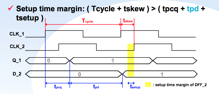
Setup time margin: $t_{cycle} + t_{skew} > t_{pcq} + t_{pd} + t_{setup}$

Setup violation => too many works in 1 cycle Apply "pipelining"
Simple inline $a = b + c$.
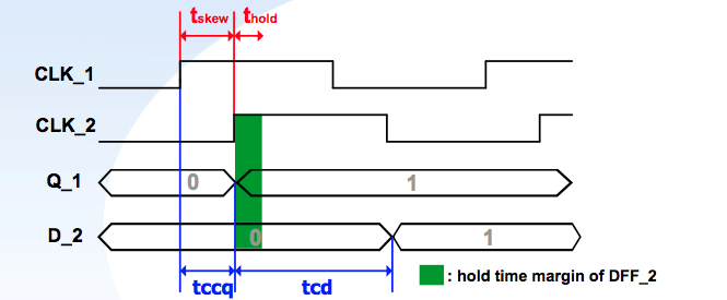
Hold time margin: $t_{ccq} + t_{tcd} > t_{hold} + t_{skew}$

Hold violation => insufficent delay
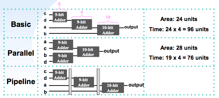
Pipe Line
Trade-off between area and timing

Lec 5
Intellectual Property (IP)
IP is a design of a logic function that specifies how the elements are interconnected.
- Soft macro IP: Synthesizable RTL
- Portable and editable
- Unknown performance, timing, area, and power
- IP protection risks
- Firm macro IP: Netlist format
- Performance optimization under specific tech
- Need not synthesizing
- Hard macro IP: Hardware (LEF, GDS2 file format)
- Physical pathways and wiring
- Moving, rotating, flipping freedom, but interior fixed
Memory - SRAM
- Read and write only
- Less area than register
- Slower than register
- One address only every access (single port)
SRAM logic table is shown below:
| CEN | OEN | WEN | Mode | Q (out) | Function |
|---|---|---|---|---|---|
| H | L | x | Standby | keep | Output remain stable |
| L | L | L | Write | A (in) | |
| L | L | H | Read | RAM data | Output at address A |
| x | H | x | High-Z | Z | operations unaffected |
For a memory having spec:
| Words | Bits |
|---|---|
| 600 | 8 |
You should use:
Data input reg [7:0] D;.
Address A reg [9:0] A;.
Lec 6
Basic Synthesis Flow
- Develop HDL files
- Specify libraries
- Synthesize in worst case
slow.db.
- Synthesize in worst case
- Read Design
read_verilog -rtl $DESIGN\.vcurrent_design $DESIGN
- Develop design environment
- Operating conditions: Process, Volt, & T
- Wire load models: Top, Enclosed, & Segmented 3 modes
To estimate capacitance, resistance and area due to interconnection.
- System interface
- Set design constraints
- Rule constraints
set_max_capacitanceset_max_transitionset_fanout_loadset_max_fanout
- Optimization contraints
- set_clock_latency
- set_clock_uncertainty
- set_propagated_clock
- set_input_delay
- set_output_delay
- Rule constraints
- Select compile strategy
- 3 compiles: Top-down, bottom-up, & mixed
- Optimize the design
compileandcompile_ultra
- Analyze and resolve design problems
check_design, like syntaxreport_areareport_timing
- Save the design database
Lec 7
Clock Latency
- Clock source latency (outside)
from clock source to clock definition point (clk) - Clock network latency (inside)
from clock definition point (clk) to clock pin of a flip-flop
Clock Domain Crossing
Data launched and captured by different(asynchronous) clock domain.
Metastability
The unstable status due to non-ideal data transition.
An example solution to CDC design, for both "fast-to-slow" and "slow-to-fast".
