Course Memo of digital IC design, including following contents:
- Low Power
- System Verilog
- Testbed Constraint and Patterns
- APR
Lec 8 - Low Power
Power Dissipation
$$P_{total} = P_{static} + P_{dynamic}$$
Static Power: $P_{static}$
Static power dissipation is caused by leakeage current.
$$P_{static} = I_{leakage} \times V_{DD}$$
Sources
- Sub-threshold $\propto T$
Donimate the leakage - Gate Leakage $\propto V_{DD}$
- Reverse Leakage $\propto T$
Happen when device is reverse biased
To minimize
- Reduce voltage supply (process dependent)
- In general the leakage current can't be changed if process and cells are decided
Dynamic Power
Dominate power dissipation.
$$P_{dynamic} = p_t \times \left( {P_D + P_{SC}} \right)$$
- $P_t$
Switching probability of clock cycle - $P_D = C_{load} \cdot V_{DD}^2 \cdot f_{clk}$
Switching power, charging and discharging the loadgin capacitance - $P_{SC} = t_{sc} \cdot V_{DD} \cdot I_{peak} \cdot f_{clk}$
Short circuit power, direct path between VDD and GND when switching, both NMOS and PMOS are turned on
To minimize
- Reduce unnecessary switching acitivities $\Rightarrow p_t$
- Gated clock (Turn off unused circuits)
- Register retiming
- State assign
- Reduce parastic capacitance $\Rightarrow P_D$
- Reduce $V_{DD}$, process dependent $\Rightarrow P_D, P_{SC}$
- Reduce the overlap time of PMOS and NMOS turn-on time. Ex: Keep the input signal rise/fall time the same. $\Rightarrow P_{SC}$
Low Power Design Methodologies
- Reduce supply VDD: Multi Voltage
- Reduce leakage current: Multi Vt
- Reduce transition frequency (activity)
Lower the clock frequency. Circuit techniques (clock gating, register retiming, …) - Reduce loading capacitance $C_{load}$ Depends on layout, material, and process.
- Reduce short circuit current
Balance the $t_{rise}$ and $t_{fall}$ of logic gate input.
Multi Voltage
Reduce VDD is though straightfoward, decreasing VDD would cause the circuit delay increasing.
- Static Voltage Scaling (SVS) Different blocks or subsystems => different fixed supply voltages
- Multi-level Voltage Scaling (MVS) A block or subsystem => switching between two or more voltage levels
- Dynamic Voltage and Frequency Scaling (DVFS) An extension of MVS where a larger # of voltage levels are dynamically switched to follow changing workloads.
A level shifter may cause:
- Timing inaccuracy
- Signals are not propagated
Challenges
- Level shifter need to be carefully designed, including the clock tree synthesis tool
- Timing analysis is more complex
- Floor planning, power planning, etc.
Multi Vt
As Vt decreases, sub-threshold leakage increases.
- Power concern: High Vt
- Delay concern: Low Vt
With multi-Vt technology, critical path uses low-Vt logic to reduce delay, and non-critical path use path-Vt to reduce power dissipation. There are mixed of defferent Vt devices in one logic gate.
Power Gating
Switching between modes to maximize power saving while minimizing the impact to performance. Power gating needs a control circuit to schedule the whole procedure.
- A low power mode
- An active mode
- Sleep mode: shut down power to block logic
Common Power Format
A TCL-based power specificatioin file, consisting of commands and objects describing power intent.
Clock Gating
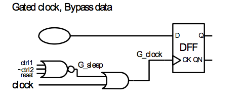
- Reduce poewr consumption of registers by turn off the unused registers.
- Reduce the clock switching power.
Methods
- Gated clock, bypasss data
For a design on ASIC. The gated conditions should be chosen carefully.

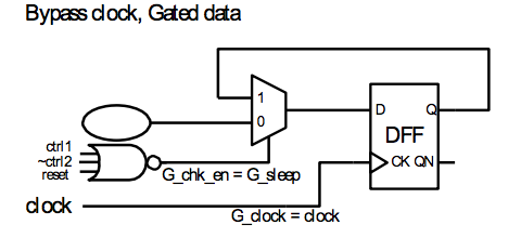
- Gated data, bypass clock
For a design on FPGA the clock tree is pre-generated, so it's difficult to implement dynamic gated clock scheme.
To logic equivalent with dynamic gated clock design, the data gating condition should be same with above.
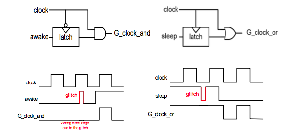
Clock gating can be implemented by either AND- or OR- gating. The control signal can only change in specific half cycle (Low period for AND gate, high period for OR gate).
Use a latch to avoid glitch.

OR-gating is better_, since the gated clock is tied at high when the register is turned off. No matter data is toggling, the first latch circuit will not be toggled.
However, for AND-gating, the fated clock is tied at low when the register is turned off. The first latch circuits will consume power as data input is switching.
The gating control signals should be generated from clock rising edge flip-flops.
- Consistent with original clock rising edge triggering design
- Easier for timing control and analysis
Lec 9 - System Verilog
Design Environment
testbed.sv
- Connecting testbench and design modules
- Generating clock
- Dump waveform
design.sv
- Design under test
pattern.sv
- Pattern
- Test program
- Assertion
- Converage
Data Types
4-State Variables 10ZX
Default is X if not initialized.
1
logic w; // used in both assignment and procedure blocks
logic
- No input and output restriction
- No continuous or block procedure restriction
1
2
reg r;
integer i; // 32-bit data type
2-State Variables 10
Defualt is 0 if not initialized.
1
2
3
4
5
bit b; // 1-bit integer
byte b_8; // 8-bit signed integer
shortint s; // 16-bit signed integer
int i; // 32-bit signed integer
longint l; // 64-bit signed integer
Enumerate
Enumerate defines a set of named values, providing built-in assertion. Default data type is int. Variables are initialized to 0 if not initialized.
1
2
3
4
5
6
enum {red, green, blue} led; // red=0, green=1, blue=2
enum logic [1:0] {A=2'b01, B=2'10, C=2'b11} class_name;
typedef enum {IDLE, WAIT, LOAD, RUN} state;
state current_state;
state next_state;
Structure
Similar to class in C language. Group related signals to enhance readability and clearly convey designer's intent.
1
2
3
4
5
6
7
8
9
10
11
12
struct {
int num;
logic[3:0] address;
} INSTRUCT;
INSTRUCT.address = 4'hff;
typedef struct {
int a,b;
state s;
} Core;
Core CPU;
CPU.state = IDLE;
Package
Package can include parameters, user-defined enumerates, structures, and functions.
1
2
3
4
5
6
7
8
9
10
11
12
13
14
15
16
17
18
19
20
21
22
23
24
25
26
27
28
29
30
31
32
33
34
package calculator;
parameter VERSION = "1.0";
typedef enum {ADD, SUB, MULT} operation;
typedef struct {
logic [31:0] a, b;
operation op;
} Instruct;
function automatic [31:0] multiple (input [31:0] in_a, in_b);
return in_a * in_b;
endfunction
endpackage
/**
* Use package in module
*/
import calculator::*;
module ALU (
// Without import, you need to use like:
// input calculator::Instruct INS
input Instruct INS,
input logic clk,
output logic[31:0] result
);
always_comb begin
case (INS.op)
ADD: result = INS.a + INS.b;
SUB: result = INS.a - INS.b;
MULT:result = multiple(INS.a, INS.b);
endcase
end
endmodule
Procedure Blocks
In Verilog, always is a general procedure block, depending on context which is not intuitive. System Verilog adds 3 new logic specific processes to show designers' intent:
- always_comb
- always_ff
- always_latch
always_comb
1
2
3
4
5
6
7
// Verilog 2001
always@(b or c)
a = b & c;
// System Verilog
always_comb
a = b & c;
always_ff
1
2
3
4
5always_ff@(posedge clk or negedge rst_n)
if(!rst_n)
q <= 0;
else
q<= d;
Interface
The interface encapsulate communication between design blocks and verifications blocks.

1
2
3
4
5
6
7
8
9
10
11
12
13
14
15
16
17
interface INF;
state s;
logic in_valid;
logic [9:0] data;
endinterface
module m_A(
input clk,
INF intf_A
);
endmodule
module main(input clk);
INF intf();
module m_A(.clk(clk), .intf_A(intf));
// other codes…
endmodule
Modports
Modports are used to define derection of signal inside interface.
1
2
3
4
5
6
7
8
9
10
11
12
13
14
15
16
17
18
19
20
21
22
23
24
25
26
27
28
29
30
31
32
33
34
35
36
37
38
39
40
41
42
43
44
45
46
47
48
49
import calculator::*;
interface INF();
logic rst;
logic [31:0] a, b, out;
operation op;
modport PATTERN(
output rst,
output op,
output a,
output b,
input out
);
modport DESIGN(
input rst,
input op,
input a,
input b,
output out
);
endinterface
/**
* In TESTBED.sv
*/
module TESTBED;
// …
INF inf();
PATTERN pattern(
.clk(clk),
.inf(inf.PATTERN)
);
ALU design(
.clk(clk),
.inf(inf.DESIGN)
);
// …
endmodule
/**
* In ALU.sv
*/
module ALU(
input clk,
INF.DESIGN inf
);
// …
endmodule
Program Block
A program differs from a module:
- Only initial blocks allowed
- Special semantics
- Execute in reactive region
Object-Oriented Programming
Contents of an object:
- Data field
- Constructor
- Methods
Randomization
Two types of random properties:
- rand
- randc
| rand | randc |
|---|---|
| Any legal value | Up to 16 bits |
| Might repeat | Cyclic repeat |
For randc bit values > 16-bits, use concatenation.
A built-in method randomize in each random class, call it to randomized data, returning 1 if successful, and 0 if randomization failed.
Constraints
Class properties are constrained in a constraint block.
1
2
3
4
5
6
7
8
9
10
11
12
13
14
15
16
17
18
19
20
21
22
23
24
25
26
27
28
29
30
31
32
program test;
class Location;
rand bit[9:0] area;
randc bit[8:0] lat;
randc bit[8:0] lang;
constraint existing {
area > 0;
lat inside {[-90, 90]};
lang inside {[-180, 180]};
}
constraint not_origin {
!(lat == 0);
!(lang== 0);
}
constraint south_east {
lat <= 0;
lang >= 0;
}
endclass
Location country;
initial begin
country = new();
if(!country.randomize())
$display("Fail to randomize.");
else
// …
end
endprogram
Generation Code: For
Useful for vector or array, generated codes are equal to printed codes.
1
2
3
4
5
6
7
8
9
10
11
12
13
genvar i;
logic [1:0] counts [0:3];
generate
for(i=0; i<4; i=i+1) begin: generate_counts
always_ff@(posedge clk) begin
if(inf.rst)
counts[i] <= 0;
else
counts[i] <= 10-i;
end
end
endgenerate
Lec 10
Coverage
Code coverages:
- Statement (line)
- Block
- Conditional expression
- Branch and dicision
- Toggle
- Finite state machine
1
2
3
4
5
6
7
8
9
10
11
12
13
14
15
16
17
18
19
covergroup coverage @(posedge clk);
A_sig: coverpoint a {
bins big = {[0:15]}; // 1 state bin
bins to_0 = ([1:511]=>0); // 1 transition bin
bins to_n [] = ([0:6]=>[9:16]); // 7*8 transition bins
ignore_bins no = {4,6};
illegal_bins fail = {512};
}
B_sig: coverpoint b;
AB_cross: cross A_sig, B_sig;
Result: coverpoint result {
// automatically 512 bins are created with equal portion
option.auto_bin_max = 512;
option.at_least = 16;
}
endgroup
coverage cov = new();
The core utilization must be decided first. Usually the core utilization is higher than 85%;
$$ core\ size\ of\ standard\ cell=\frac{standard\ cell\ area}{core\ utilization}$$
Core Margins leave the space for power/ground rings.
$$ die\ size=min(pad\ total\ width, core\ width+core\ margin) $$
It is called max(pad, core) limited design.
Pad fillers provide power to pad and there should be no spacing between pads. Pad fillers are necessary for core limited design.
Powerplan
Issues
-
Metal migration
Or electro-migration. Under high current => open or short due to electron collisions with metal grains.Prevention: Sizing power supply lines to ensure chip does not fail.
Expereince: Make sure current density of power ring < 1mA/µm.
-
IR drop Device runs at slower speed if IR drop, causing slower performance, setup/hold violations, less noise margin, and leakage power, is excessive.
Prevention: Adding stripes.
Core power ring
1
2
3
4
5
6
7
8
9
10
11
12
13
14
15
16
| No Wire Group | Wire Group |
--------------|---------------|---------------|
| | |
| x–––––––– VDD | x–x–––––– VDD |
No | | x–––––– VDD | x–x–––––– VDD |
Interleaving | | | x–––– gnd | | | x–x–– gnd |
| | | | x–– gnd | | | x–x–– gnd |
| | | | | | | | | | |
--------------|---------------|---------------|
| | |
| x–––––––– VDD | x–––x–––– VDD |
| | x–––––– gnd | | x–+–x–– gnd |
Interleaving | | | x–––– VDD | x +–x–+–– VDD |
| | | | x–– gnd | | x–+–x–– gnd |
| | | | | | | | | | |
--------------|---------------|---------------|
Standard Cell Placement
CTS
Clock tree synthesis
Clock problems:
- Heavy clock net loading
- Long clock insertion delay
- Clock skew
- Skew across clocks
- Clock to signal coupling effect
- Power hungry
- Electomigration on clock net
Routing
Signal integrity (SI) issues:
- Corsstalk
- Charge sharing
- Supply noise
- Leakage
- Propagated noise
- Overshoot
- Under shoot
SI deiven route
Crosstalk preventions:
- Placement solution
- Insert buffer in lines
- Upsize driver
- Congestion optimization
- Routing solution
- Limit length of parallel or reducing nets
- Wider wiring spacing
- Shield special nets
- Layer switching
Antenna effect
In a chip manufacturing process, metal is initially deposited so it covers the entire chip. Then, the unneeded portions of the metal are removed by etching, typically in plasma (charged particles). The exposed metal collect charge from plasma and form voltage potential. If the voltage potential across the gate oxide becomes large enough, the current can damage the gate oxide.
$$ antenna\ ratio=\frac{area\ of\ process\ antennas\ on\ a\ node}{area\ of\ gates\ to\ node}$$
Repairments:
- Add jumper
- Add antenna cell (diode)
- Add buffer
Lec 12 - APR II
LEF defines the elements of an IC process technology and associated library of cell models.
- Technology LEF Containing information like placement, routing design rules, and process information for layers.
- Cell library LEF Containing the macro and standard cell information for a design.